Device Library Catalog
Basic components
cap: Linear Capacitor
Connection diagram:
             || C
0 o----------||---------o 1
             ||
Netlist example:
cap:c1 1 2 c=10uF
Parameters
Name Default Unit Description c 0.0 F Capacitance
ind: Inductor
Connection diagram:
         __  __  __  _
0       /  \/  \/  \/ \          1
  o----+   /\  /\  /\  +-------o    External view
          (_/ (_/ (_/
Netlist example:
ind:l1 1 0 l=3uH
Internal Topology
Internal implementation uses a gyrator (adds il internal node):
                                il/gyr    Term: il
0  o---------+            +----------------+
             | gyr V(il)  |                |
  +         /|\          /^\               |
Vin        ( | )        ( | ) gyr Vin    ----- gyr^2 * L
  -         \V/          \|/             -----
             |            |                |
1  o---------+            +----------------+
                                  |
                                 --- tref
                                  V
Parameters
Name Default Unit Description l 0.0 H Inductance
memd: Memductor
Connection diagram:
          +  Vin   -      Iin
        _______________  ---->
0      |_   _   _   _| |         1
  o----| |_| |_| |_| | |-------o    External view
       |_____________|_|
Device equation:
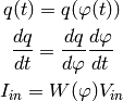
 is the memductance function.
Netlist example:
memd:m1 1 0 w = '1e3 * (np.cosh(1e6 * phi)-1.)'
Notes:
- the memductance function (W(phi)) is given as an expression in the w parameter. The independent variable is the memductor flux: phi. Constants and mathematical functions can also be used in the definition of w.
- The initial flux can be adjusted with the phi0 parameter
- the memductor loses its memory as the capacitor discharges through Rleak (Rleak is necessary to ensure a unique DC solution). The values of C and Rleak can be adjusted to change the time constant
- The capacitor value has no effect on the memductance, but has an effect in the internal model: a larger capacitor will produce lower voltages at vc.
Internal Topology
The internal implementation uses a gyrator and adds one internal node: vc. The voltage at vc is equal to (gyr/C) * phi, where gyr is a global variable that can be changed with the .options keyword:
      --> Iin
0  o---------+
             |
  +         /|\  i = w(phi) * Vin
Vin        ( | )
  -         \V/  phi = (C/gyr) * vc
             |
1  o---------+

                             Term: vc
+       +----------------+--------+---------,
        |                |        |         |
       /^\             -----      /        /^\
vc    ( | ) gyr Vin    ----- C    \ Rleak ( | ) phi0 * gyr / C / Rleak
       \|/               |        /        \|/
        |                |        |         |
-       +----------------+--------+---------'
                         |
                        --- tref
                         -
Parameters
Name Default Unit Description c 1e-05 F Auxiliary capacitance phi0 0.0 Vs Initial flux rleak 1000000000.0 Ohms Leackage resistance w abs(1e-3*phi) Siemens Memductance function W(phi)
memr: Memristor
Connection diagram:
          +  Vin   -      Iin
        _______________  ---->
0      |_   _   _   _| |         1
  o----| |_| |_| |_| | |-------o    External view
       |_____________|_|
Device equation:
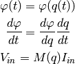
 is the memristance function.
Netlist example:
memr:m1 1 0 m = '1e3 * (np.cosh(1e6 * q)-1.)'
Notes:
- the memristance function (M(q)) is given as an expression in the m parameter. The independent variable is the memristor charge (q). Constants and mathematical functions can also be used in the definition.
- The initial charge can be adjusted with the q0 parameter
- the memristor loses its memory as the capacitor discharges through Rleak (Rleak is necessary to ensure a unique DC solution). The values of C and Rleak can be adjusted to change the time constant
- The capacitor value has no effect on the memristance, but has an effect in the internal model: a larger capacitor will produce lower voltages at vc.
Internal Topology
The internal implementation uses a gyrator and adds 2 internal nodes: im and vc. The voltages at those terminals have the following meaning (gyr is a global variable that can be changed with the .options keyword):
im: Iin / gyr
vc: q / C

      --> Iin                          Term: im
0  o---------+            +----------------+
             | gyr V(im)  |                |
  +         /|\          /^\              /|\
Vin        ( | )        ( | ) gyr Vin    ( | ) gyr^2 * M(q) * V(im)
  -         \V/          \|/              \V/
             |            |                |   q = C * vc
1  o---------+            +----------------+
                                  |
                                 --- tref
                                  -

                             Term: vc
+       +----------------+--------+---------,
        |                |        |         |
       /^\             -----      /        /^\
vc    ( | ) gyr V(im)  ----- C    \ Rleak ( | ) q0 / C / Rleak
       \|/               |        /        \|/
        |                |        |         |
-       +----------------+--------+---------'
                         |
                        --- tref
                         -
Parameters
Name Default Unit Description c 1e-05 F Auxiliary capacitance m abs(5e9*q) Ohms Memristance function M(q) q0 0.0 As Initial charge rleak 1000000000.0 Ohms Leackage resistance
res: Resistor
Connection diagram:
              R
0 o--------/\/\/\/---------o 1
Normally a linear device. If the electro-thermal version is used (res_t), the device is nonlinear.
Netlist examples:
# Linear resistor (2 terminals)
res:r1 1 2 r=1e3 tc1=10e-3

# Electro-thermal resistor (nonlinear, 4 terminals)
res_t:r1 1 2 3 4 r=1e3 tc1=10e-3
Parameters
Name Default Unit Description l 0.0 m Length narrow 0.0 m Narrowing due to side etching r 0.0 Ohms Resistance rsh 0.0 Ohms Sheet resistance tc1 0.0 1/C Temperature coefficient 1 tc2 0.0 1/C^2 Temperature coefficient 2 temp None C Device temperature (None: use global temp.) tnom 27.0 C Nominal temperature w 0.0 m Width
Electro-thermal version
Electro-thermal version with extra thermal port: res_t
Controlled Sources
gyr: Gyrator
The gyrator converts Port 1 voltage into Port 2 current and vice-versa. Combined with the VCCS device it can be used to implement all the remaining controlled sources:
- VCVS = VCCS + gyrator
- CCCS = gyrator + VCCS
- CCVS = gyrator + VCCS + gyrator
Connection diagram:
     0  o---------+            +----------o 2
 +                |            |                +
                 /|\          /^\
Vin1     g Vin2 ( | )        ( | ) g Vin1      Vin2
                 \V/          \|/
 -                |            |                -
     1  o---------+            +----------o 3
Netlist example:
gyr:gg 1 0 2 0 g=1m
Parameters
Name Default Unit Description g 0.001 Ohms Gyrator gain
vccs: Voltage-controlled current source
Schematic:
           g Vc   (or if nonlinear, i(vc))
           ,---,
0 o-------( --> )---------o 1
           `---`


2 o      +  Vc   -        o 3
By default the source is linear. If a nonlinear function is provided, the linear gain (g) is not used and must not be specified in the netlist.
Netlist examples:
vccs:g1 gnd 4 3 gnd g=2mS
vccs:iout 0 cout 1 0 f='1e-3 * np.tanh(vc)'
Parameters
Name Default Unit Description f A Nonlinear function i(vc) g 0.001 S Linear transconductance
Distributed components
tlinps4: 4-Terminal Physical Transmission Line
This model uses scattering parameters:
0 o===================================o 2
                  Z0
1 o===================================o 3
This model is similar to tlinpy4, but it is more robust and can
handle lossless lines, even at DC, but internally requires 2
additional ports to keep track of  and
and
 . This model is more suitable for convolution as the S
parameters are better behaved than the Y parameters.
. This model is more suitable for convolution as the S
parameters are better behaved than the Y parameters.
Netlist Examples:
tlinps4:tl1 in gnd out gnd z0mag=100. length=0.3m
.model c_line tlins4 (z0mag=75.00 k=7 fscale=1.e10 alpha = 59.9)
Internal Topology
The model is symmetric. The schematic for Port 1 is shown here:
         I1                              v1+ + v1-  Term:   v1-
        --->                               ---->     v1p   ---->
    0 o--------,                          ,------------+----------,  4
 +             |                          |            |          |
               |                          |           ,-,  s12 v2+|
V1            /|\ (v1+ - s12 v2+)/Z0     /^\          | |        /|\
             ( | )                      ( | )       1 | |       ( | )
 -            \V/                    V1  \|/          '-'        \V/
               |                          |            |          |
    1 o--------+                          +---------+--+----------'
                                                    |
                                                   --- lref (6)
                                                    V
Internal terminal names: v1p (keeps track of ) and v1m
(keeps track of  )
)
Note: for a matched transmission line, s11 = s22 = 0 and s12 = s21. The equivalent ‘Y’ matrix is:
    |              1/Z0    -s12/Z0 |
    |                              |
    |             -s21/Z0    1/Z0  |
Y = |                              |
    | -1            1        s12   |
    |                              |
    |        -1    s21        1    |
Parameters
Name Default Unit Description alpha 0.1 dB/m Attenuation fscale 0.0 Hz Scaling frequency for attenuation k 1.0 Effective relative dielectric constant length 0.1 m Line length tand 0.0 Loss tangent z0mag 50.0 Ohms Magnitude of characteristic impedance
tlinpy4: 4-Terminal Physical Transmission Line
This model uses Y parameters:
0 o===================================o 2
                  Z0
1 o===================================o 3
Code derived from fREEDA tlinp4 element. fREEDA implementation by Carlos E. Christoffersen, Mete Ozkar, Michael Steer
Two models are supported dependent on the secting of nsect: When nsect = 0 (not set) the frequency-domain model is enabled. When nsect > 0 the transmission line is expanded in nsect RLCG subsections.
Netlist Examples:
tlinpy4:tl1 in gnd out gnd z0mag=100. length=0.3m
.model c_line tlinpy4 (z0mag=75.00 k=7 fscale=1.e10 alpha = 59.9)
Internal Topology
The internal schematic when nsect = 0 is the following:
    0 o----+------,               ,-----+-------o 2
 +         |      |               |     |              +
          ,-,     |               |    ,-,
v1        | |    /|\ y12 v2      /|\   | |             v2
      y11 | |   ( | )           ( | )  | | y22
 -        '-'    \V/      y21 v1 \V/   '-'             -
           |      |               |     |
    1 o----+------'               '-----+-------o 3

                 y11 = y22 , y12 = y21
Parameters
Name Default Unit Description alpha 0.1 dB/m Attenuation fopt 0 Hz Optimum frequency for discrete approximation fscale 0.0 Hz Scaling frequency for attenuation k 1.0 Effective relative dielectric constant length 0.1 m Line length nsect 0 Enable discrete approximation with n sections tand 0.0 Loss tangent z0mag 50.0 Ohms Magnitude of characteristic impedance
Semiconductor devices
acm_i: Incomplete Intrinsic ACM MOSFET
Only (some) DC equations are implemented for now. Temperature dependence is not complete. Terminal order: 0 Drain, 1 Gate, 2 Source, 3 Bulk:
         Drain 0
                 o
                 |
                 |
             |---+
             |
Gate 1 o-----|<-----o 3 Bulk
             |
             |---+
                 |
                 |
                 o
        Source 2
Netlist examples:
acm_i:m1 2 3 4 gnd w=10e-6 l=1e-6 type = n
acm_i:m2 4 5 6 6 w=30e-6 l=1e-6 type = p
Internal topology
For now only ids is implemented:
                 ,--o 0 (D)
                 |
                 |
                 |
                 |
                /|\
(G) 1 o-       ( | ) ids(VD, VG, VS, VB)
                \V/
                 |
                 |
                 |
                 |
(B) 3 o-         `--o 2 (S)
Parameters
Name Default Unit Description gamma 0.631 V^(1/2) Bulk Threshold Parameter kp 0.0005106 A/V^2 Transconductance Parameter l 1e-05 m Channel length phi 0.55 V Surface Potential temp None C Device temperature (None: use global temp.) theta 0.814 1/V Mobility Saturation Parameter tnom 27.0 C Nominal temperature of model parameters tox 7.5e-09 m Oxide Thickness type n N- or P-channel MOS (n or p) vsat 80000.0 m/s Saturation Velocity vt0 0.532 V Threshold Voltage w 1e-05 m Channel width
Electro-thermal version
Electro-thermal version with extra thermal port: acm_i_t
acms_i: Simplified ACM Intrinsic MOSFET
This model uses the simple equations for hand analysis. Only DC equations (with temperature dependence) included for now.
Terminal order: 0 Drain, 1 Gate, 2 Source, 3 Bulk:
         Drain 0
                 o
                 |
                 |
             |---+
             |
Gate 1 o-----|<-----o 3 Bulk
             |
             |---+
                 |
                 |
                 o
        Source 2
Netlist examples:
acms_i:m1 2 3 4 gnd w=10e-6 l=1e-6 type = n
acms_i:m2 4 5 6 6 w=30e-6 l=1e-6 type = p
Internal topology
Only ids is implemented. In the future charges will be added:
                 ,--o 0 (D)
                 |
                 |
                 |
                 |
                /|\
(G) 1 o-       ( | ) ids(VD, VG, VS, VB)
                \V/
                 |
                 |
                 |
                 |
(B) 3 o-         `--o 2 (S)
Parameters
Name Default Unit Description bex -1.5 Mobility temperature exponent cox 0.0007 F/m^2 Gate oxide capacitance per area isq 1e-07 A/V^2 Sheet normalization current l 1e-05 m Channel length n 1.3 F/m^2 Subthreshold slope factor tcv 0.001 V/K Threshold voltage temperature coefficient temp None C Device temperature (None: use global temp.) tnom 27.0 C Nominal temperature of model parameters type n N- or P-channel MOS (n or p) vth 0.5 V Threshold Voltage w 1e-05 m Channel width
Electro-thermal version
Electro-thermal version with extra thermal port: acms_i_t
bjt: Bipolar Junction Transistor
This device accepts 3 or 4 terminal connections.
Netlist examples:
bjt:q1 2 3 4 1 model = mypnp isat=4e-17 bf=147 iss=10fA
bjt:q2 2 3 4  model = mypnp isat=4e-17 bf=147 vaf=80 ikf=4m
svbjt:q3 2 3 4 1 model = mypnp vaf=80 ikf=4m iss=15fA

# Electro-thermal versions
bjt_t:q2 2 3 5 1 pout gnd model = mypnp
svbjt_t:q3 2 3 5 1 pout gnd model = mypnp

# Model statement
.model mypnp bjt_t (type=pnp isat=5e-17 cje=60fF vje=0.83 mje=0.35)
Extrinsic Internal Topology
RC, RE and a Collector-Bulk connection are added to intrinsic BJT models:
            RC    Term: ct      Term: et   RE
C (0) o---/\/\/\/--+-----,         4----/\/\/\/----o  E (2)
                   |      \       /
                   |       \     /
                 -----    ---------
                  / \         |
                 /   \        o
                 -----
                   |          B (1)
                   o Bulk (3)
If RE or RC are zero the internal nodes (ct, et) are not created. If only 3 connections are specified then the Bulk-Collector junction is not connected.
Important Note
This implementation does not account for the power dissipation in RE, RC. Use external thermal resistors if that is needed.
Intrinsic Model Information
Gummel-Poon intrinsic BJT model
This implementation based mainly on previous implementation in carrot and some equations from Pspice manual.
Terminal order: 0 Collector, 1 Base, 2 Emitter:
C (0) o----,         4----o  E (2)
            \       /
             \     /
            ---------
                |
                o

                B (1)
Can be used for NPN or PNP transistors.
Intrinsic Internal Topology
Internally may add 2 additional nodes (plus reference) if rb is not zero: Bi for the internal base node and tib to measure the internal base current and calculate Rb(ib). The possible configurations are described here.
If RB == 0:
                +----------------+--o 0 (C)
                |                |
               /^\               |
              ( | ) ibc(vbc)     |
               \|/               |
                |               /|\
(B) 1 o---------+              ( | ) ice
                |               \V/
               /|\               |
              ( | ) ibe(vbe)     |
               \V/               |
                |                |
                +----------------+--o 2 (E)
If RB != 0:
                            +----------------+--o 0 (C)
                            |                |
                           /^\               |
                          ( | ) ibc(vbc)     |
           gyr * tib       \|/               |
            ,---,           |               /|\
(B) 1 o----( --> )----------+ Term : Bi    ( | ) ice
            `---`           |               \V/
                           /|\               |
                          ( | ) ibe(vbe)     |
                           \V/               |
                            |                |
                            +----------------+--o 2 (E)
            gyr v(1,Bi)
             ,---,
        +---( <-- )------+
        |    `---`       |
 tref   |                | voltage: ib/gyr
    ,---+                |
    |   |    ,---,       |
    |   +---( --> )------+ Term : ib
    |        `---`
   ---     gyr ib Rb(ib)
    V
Charge sources are connected between internal nodes defined above. If xcjc is not 1 but RB is zero, xcjc is ignored.
Parameters
Name Default Unit Description area 1.0 Current multiplier bf 100.0 Ideal maximum forward beta br 1.0 Ideal maximum reverse beta cjc 0.0 F Base collector zero bias p-n capacitance cje 0.0 F Base emitter zero bias p-n capacitance cjs 0.0 F Collector substrate capacitance eg 1.11 eV Badgap voltage fc 0.5 Forward bias depletion capacitor coefficient ikf 0.0 A Forward-beta high current roll-off knee current ikr 0.0 A Corner for reverse-beta high current roll off irb 0.0 A Current at which rb falls to half of rbm isat 1e-16 A Transport saturation current isc 0.0 A Base collector leakage saturation current ise 0.0 A Base-emitter leakage saturation current iss 1e-14 A Substrate saturation current itf 0.0 A Transit time dependency on ic mjc 0.33 Base collector p-n grading factor mje 0.33 Base emitter p-n grading factor mjs 0.0 substrate junction exponential factor nc 2.0 Base-collector leakage emission coefficient ne 1.5 Base-emitter leakage emission coefficient nf 1.0 Forward current emission coefficient nr 1.0 Reverse current emission coefficient ns 1.0 substrate p-n coefficient rb 0.0 Ohm Zero bias base resistance rbm 0.0 Ohm Minimum base resistance rc None Ohm Collector ohmic resistance re None Ohm Emitter ohmic resistance temp None C Device temperature (None: use global temp.) tf 0.0 s Ideal forward transit time tnom 27.0 C Nominal temperature tr 0.0 s Ideal reverse transit time type npn Type (npn or pnp) vaf 0.0 V Forward early voltage var 0.0 V Reverse early voltage vjc 0.75 V Base collector built in potential vje 0.75 V Base emitter built in potential vjs 0.75 V substrate junction built in potential vtf 0.0 V Transit time dependency on vbc xcjc 1.0 Fraction of cbc connected internal to rb xtb 0.0 Forward and reverse beta temperature coefficient xtf 0.0 Transit time bias dependence coefficient xti 3.0 IS temperature effect exponent
Electro-thermal version
Electro-thermal version with extra thermal port: bjt_t
bsim3_i: Intrinsic BSIM3 MOSFET Model (version 3.2.4)
This model mainly converted from fREEDA 2.0 mosnbsim3 model written by Ramya Mohan (http://www.freeda.org/) with some improvements. Also includes some code taken from ngspice (http://ngspice.sourceforge.net/) and pyEDA EDA Framework (https://github.com/cogenda/pyEDA). Results are reasonable but requires more testing
Default parameters listed for NMOS type. Default values for some parameters such as u0 and vth0 are different for PMOS type.
Notes:
- Most parameters are not checked for valid values
- According to ngspice documentation, temperature specification is not functional (probably the same applies here)
- Parameter descriptions need reviewing
- The code to internally calculate k1 and k2 is disabled by default because using default values seems to give more reasonable results (use k1enable to enable).
Terminal order: 0 Drain, 1 Gate, 2 Source, 3 Bulk:
         Drain 0
                 o
                 |
                 |
             |---+
             |
Gate 1 o-----|<-----o 3 Bulk
             |
             |---+
                 |
                 |
                 o
        Source 2
Netlist examples:
bsim3_i:m1 2 3 4 gnd w=10e-6 l=1e-6 type = n
bsim3_i:m2 4 5 6 6 w=30e-6 l=1e-6 type = p
Internal topology
The internal topology is the following:
        ,----------------------------+-------------+--o 0 (D)
        |                            |             |
       /|\                           |             |
      ( | ) idb (Vds > 0)          -----           |
       \V/                         ----- qd        |
        |             1 (G)          |            /|\
        |               o            |           ( | ) ids
        |               |            |            \V/
        |               |            |             |
        |             -----          |             |
        |             ----- qg       |      qs     |
        |               |            |      ||     |
(B) 3 o-+---------------+------------+------||-----+--o 2 (S)
                                            ||
Parameters
Name Default Unit Description a0 1 Non-uniform depletion width effect coefficient a1 0 Non-saturation effect coefficient a2 1 Non-saturation effect coefficient acde 1 Exponential coefficient for finite charge thickness ags 0 Gate bias coefficient of Abulk alpha0 0 m/V Substrate current model parameter alpha1 0 V^{-1} Substrate current model parameter at 33000 m/s Temperature coefficient of vsat b0 0 Abulk narrow width parameter b1 0 Abulk narrow width parameter beta0 30 V Diode limiting current cdsc 0.00024 F/m^2 Drain/Source and channel coupling capacitance cdscb 0 F/V/m^2 Body-bias dependence of cdsc cdscd 0 F/V/m^2 Drain-bias dependence of cdsc cit 0 Interface state capacitance clc 1e-07 Vdsat paramater for C-V model cle 0.6 Vdsat paramater for C-V model delta 0.01 V Effective Vds parameter drout 0.56 DIBL coefficient of output resistance dsub 0.56 DIBL coefficient in the subthreshold region dvt0 2.2 Short channel effect coefficient 0 dvt0w 0 m^{-1} Narrow width effect coefficient 0 dvt1 0.53 Short channel effect coefficient 1 dvt1w 5300000.0 m^{-1} Narrow width effect coefficient 1 dvt2 -0.032 V^{-1} Short channel effect coefficient 2 dvt2w -0.032 V^{-1} Narrow width effect coefficient 2 dwb 0 m/V Width reduction parameter dwg 0 m/V Width reduction parameter elm 5 Non-quasi-static Elmore Constant Parameter eta0 0.08 Subthreshold region DIBL coefficeint etab -0.07 Subthreshold region DIBL coefficeint k1 0.53 V^{0.5} First order body effect coefficient k1enable 0 Enable k1, k2 internal calculation k2 -0.0186 Second order body effect coefficient k3 80 Narrow width effect coefficient k3b 0 Body effect coefficient of k3 keta -0.047 Body-bias coefficient of non-uniform depletion width effect kt1 -0.11 V Temperature coefficient of Vth kt1l 0 V m Temperature coefficient of Vth kt2 0.022 Body-coefficient of kt1 l 1e-06 m Length lint 0 m Length reduction parameter ll 0 Length reduction parameter llc 0 Length reduction parameter for CV lln 1 Length reduction parameter lw 0 Length reduction parameter lwc 0 Length reduction parameter for CV lwl 0 Length reduction parameter lwlc 0 Length reduction parameter for CV lwn 1 Length reduction parameter moin 15 Coefficient for gate-bias dependent surface potential nch 1.7e+17 cm^{-3} Channel doping concentration nfactor 1 Subthreshold swing coefficient ngate 0 cm^{-3} Poly-gate doping concentration nlx 1.74e-07 m Lateral non-uniform doping effect noff 1 C-V turn-on/off parameter nsub 6e+16 cm^{-3} Substrate doping concentration pclm 1.3 Channel length modulation coefficient pdibl1 0.39 Drain-induced barrier lowering oefficient pdibl2 0.0086 Drain-induced barrier lowering oefficient pdiblb 0 Body-effect on drain induced barrier lowering prt 0 Temperature coefficient of parasitic resistance prwb 0 Body-effect on parasitic resistance prwg 0 Gate-bias effect on parasitic resistance pscbe1 424000000.0 V/m Substrate current body-effect coeffiecient 1 pscbe2 1e-05 V/m Substrate current body-effect coeffiecient 2 pvag 0 Gate dependence of output resistance parameter rdsw 0 Sorce-drain resistance per width temp None C Device temperature (None: use global temp.) tnom 27.0 C Nominal temperature tox 1.5e-08 m Gate oxide thickness toxm 1.5e-08 Gate oxide thickness used in extraction type n N- or P-channel MOS (n or p) u0 670 cm^2/V/s Low-field mobility at Tnom ua 2.25e-09 m/V Linear gate dependence of mobility ua1 4.31e-09 m/V Temperature coefficient for ua ub 5.87e-19 (m/V)^2 Quadratic gate dependence of mobility ub1 -7.61e-18 (m/V)^2 Temperature coefficient for ub uc -4.65e-11 m/V^2 Body-bias dependence of mobility uc1 -5.6e-11 m/V^2 Temperature coefficient for uc ute -1.5 Temperature coefficient of mobility vbm -3 V Maximum body voltage vfb -1 V Flat band voltage voff -0.08 V Threshold voltage offset voffcv 0 C-V lateral shift parameter vsat 80000 m/s Saturationvelocity at tnom vth0 0.7 V Threshold voltage of long channel device at Vbs=0 and small Vds w 1e-06 m Width w0 2.5e-06 m Narrow width effect parameter wint 0 m Width reduction parameter wl 0 Width reduction parameter wlc 0 Width reduction parameter for CV wln 1 Width reduction parameter wr 1 Width dependence of rds ww 0 Width reduction parameter wwc 0 Width reduction parameter for CV wwl 0 Width reduction parameter wwlc 0 Width reduction parameter for CV wwn 1 Width reduction parameter xj 1.5e-07 m Junction depth xt 1.55e-07 m Doping depth
diode: Junction Diode
Based on the Spice model. Connection diagram:
  o  1
  |
--+--
 / \
'-+-'
  |
  o  0
Includes depletion and diffusion charges.
Netlist examples:
diode:d1 1 0 isat=10fA cj0=20fF

# Electrothermal device
diode_t:d2 2 3 1000 gnd cj0=10pF tt=1e-12 rs=100 bv = 4.

# Model statement
.model dmodel1 diode (cj0 = 10pF tt=1ps)
Internal Topology
The internal representation is the following:
0  o
   |
   \
   / Rs
   \
   /
   |   Term : t2
   o---------,-------------,
             | i(vin)      |
  +         /|\          ----- q(vin)
vin        | | |         -----
  -         \V/            |
             |             |
1  o---------'-------------'
Terminal t2 not present if Rs = 0
Important Note
This implementation does not account for the power dissipation in Rs. Use an external thermal resistor if that is needed.
Parameters
Name Default Unit Description af 1.0 Flicker noise exponent area 1.0 Area multiplier bv inf V Breakdown voltage cj0 0.0 F Zero-bias depletion capacitance eg0 1.11 eV Energy bandgap fc 0.5 Coefficient for forward-bias depletion capacitance ibv 1e-10 A Current at reverse breakdown voltage isat 1e-14 A Saturation current kf 0.0 Flicker noise coefficient m 0.5 PN junction grading coefficient n 1.0 Emission coefficient rs 0.0 Ohms Series resistance temp None C Device temperature (None: use global temp.) tnom 27.0 C Nominal temperature tt 0.0 s Transit time vj 1.0 V Built-in junction potential xti 3.0 Is temperature exponent
Electro-thermal version
Electro-thermal version with extra thermal port: diode_t
ekv_i: Intrinsic EPFL EKV 2.6 MOSFET
Terminal order: 0 Drain, 1 Gate, 2 Source, 3 Bulk:
         Drain 0
                 o
                 |
                 |
             |---+
             |
Gate 1 o-----|<-----o 3 Bulk
             |
             |---+
                 |
                 |
                 o
        Source 2
Mostly based on [1], but some updates from a later revision (dated 1999) are also included.
[1] The EPFL-EKV MOSFET Model Equations for Simulation, Technical Report, Model Version 2.6, June, 1997, Revision I, September, 1997, Revision II, July, 1998, Bucher, Christophe Lallement, Christian Enz, Fabien Theodoloz, Francois Krummenacher, Electronics Laboratories, Swiss Federal Institute of Technology (EPFL), Lausanne, Switzerland
This implementation includes accurate current interpolation function (optional), works for negative VDS and includes electrothermal model, DC operating point paramenters and noise equations.
Code originally based on fREEDA 1.4 implementation <http://www.freeda.org>:
// Element information
ItemInfo Mosnekv::einfo =
{
  "mosnekv",
  "EPFL EKV MOSFET model",
  "Wonhoon Jang",
  DEFAULT_ADDRESS"transistor>mosfet",
  "2003_05_15"
};
Parameter limit checking, simple capacitance calculations for operating point are not yet implemented.
Netlist examples:
ekv_i:m1 2 3 4 gnd w=30e-6 l=1e-6 type = n ekvint=0

# Electro-thermal version
ekv_i_t:m1 2 3 4 gnd 1000 gnd w=30e-6 l=1e-6 type = n

# Model statement
.model ekvn ekv_i (type = n kp = 200u theta = 0.6)
Internal Topology
The internal topology is the following:
        ,----------------------------+-------------+--o 0 (D)
        |                            |             |
       /|\                           |             |
      ( | ) idb (Vds > 0)          -----           |
       \V/                         ----- qd        |
        |             1 (G)          |            /|\
        |               o            |           ( | ) ids
        |               |            |            \V/
        |               |            |             |
        |             -----          |             |
        |             ----- qg       |      qs     |
        |               |            |      ||     |
(B) 3 o-+---------------+------------+------||-----+--o 2 (S)
                                            ||
The impact ionization current (idb) is normally added to the drain current, but if the device is in reverse (Vds < 0 for N-channel) mode, it is added to the source current.
Parameters
Name Default Unit Description Lambda 0.5 Channel-length modulation af 1.0 Flicker noise exponent agamma 0.0 V^(1/2)m Area related body effect mismatch parameter akp 0.0 m Area related gain mismatch parameter avto 0.0 Vm Area related threshold voltage mismatch parameter bex -1.5 Mobility temperature exponent cox 0.0007 F/m^2 Gate oxide capacitance per area dl 0.0 m Channel length correction dw 0.0 m Channel width correction e0 1e+12 V/m Mobility reduction coefficient ekvint 0 Interpolation function (0: accurate, 1: simple) gamma 1.0 V^1/2 Body effect parameter iba 0.0 1/m First impact ionization coefficient ibb 300000000.0 V/m Second impact ionization coefficient ibbt 0.0009 1/K Temperature coefficient for IBB ibn 1.0 Saturation voltage factor for impact ionization kf 0.0 Flicker noise coefficient kp 5e-05 A/V^2 Transconductance parameter l 1e-06 m Gate length leta 0.1 Short-channel effect coefficient lk 2.9e-07 m Reverse short channel effect characteristic length np 1.0 Parallel multiple device number ns 1.0 Serial multiple device number nsub None 1/cm^3 Channel doping phi 0.7 V Bulk Fermi potential q0 0.0 A.s/m^2 Reverse short channel effect peak charge density satlim 54.5982 Ratio defining the saturation limit if/ir tcv 0.001 V/K Threshold voltage temperature coefficient temp None C Device temperature (None: use global temp.) theta 0.0 1/V Mobility recuction coefficient tnom 27.0 C Nominal temperature of model parameters tox None m Oxide thickness type n N- or P-channel MOS (n or p) u0 None cm^2/(V.s) Low-field mobility ucex 0.8 Longitudinal critical field temperature exponent ucrit 2000000.0 V/m Longitudinal critical field vfb None V Flat-band voltage vmax None m/s Saturation velocity vt0 0.5 V Long_channel threshold voltage w 1e-06 m Gate width weta 0.25 Narrow-channel effect coefficient xj 1e-07 m Junction depth
Electro-thermal version
Electro-thermal version with extra thermal port: ekv_i_t
mesfetc: Cubic Curtice-Ettemberg Intrinsic MESFET Model
Model derived from fREEDA 1.4 MesfetCT model adapted to re-use junction code from diode.py. Some parameter names have been changed: isat, tau. Uses symmetric diodes and capacitances. Works in reversed mode.
Terminal order: 0 Drain, 1 Gate, 2 Source:
         Drain 0
                 o
                 |
                 |
             |---+
             |
Gate 1 o---->|
             |
             |---+
                 |
                 |
                 o
        Source 2
Netlist example:
mesfetc:m1 2 3 4 a0=0.09910 a1=0.08541 a2=-0.02030 a3=-0.01543
Internal Topology:
           ,----------------,------------,--o 0 (D)
           |                |            |
          /^\               |            |
         ( | ) igd(Vgd)   ----- Cgd      |
          \|/             -----          |
           |                |           /|\
(G) 1 o----+----------------,          ( | ) ids(Vgs, Vgd)
           |                |           \V/
          /|\               |            |
         ( | ) igs(Vgs)   ----- Cgs      |
          \V/             -----          |
           |                |            |
           `----------------'------------'--o 2 (S)
Parameters
Name Default Unit Description a0 0.1 A Drain saturation current for Vgs=0 a1 0.05 A/V Coefficient for V1 a2 0.0 A/V^2 Coefficient for V1^2 a3 0.0 A/V^3 Coefficient for V1^3 area 1.0 Area multiplier avt0 0.0 1/K Pinch-off voltage (VP0 or VT0) linear temp. coefficient beta 0.0 1/V V1 dependance on Vds bvt0 0.0 1/K^2 Pinch-off voltage (VP0 or VT0) quadratic temp. coefficient cgd0 0.0 F Gate-drain Schottky barrier capacitance for Vgd=0 cgs0 0.0 F Gate-source Schottky barrier capacitance for Vgs=0 eg0 0.8 eV Barrier height at 0 K fcc 0.5 V Forward-bias depletion capacitance coefficient gama 1.5 1/V Slope of drain characteristic in the linear region ib0 0.0 A Breakdown current parameter isat 0.0 A Diode saturation current mgd 0.5 Gate-drain grading coefficient mgs 0.5 Gate-source grading coefficient n 1.0 Diode ideality factor nr 10.0 Breakdown ideality factor tau 0.0 s Channel transit time tbet 0 1/K BETA power law temperature coefficient temp None C Device temperature (None: use global temp.) tm 0.0 1/K Ids linear temp. coeff. tme 0.0 1/K^2 Ids power law temp. coeff. tnom 27.0 C Nominal temperature vbd inf V Breakdown voltage vbi 0.8 V Built-in potential of the Schottky junctions vds0 4.0 V Vds at which BETA was measured vt0 -inf V Voltage at which the channel current is forced to be zero for Vgs<=Vto xti 2.0 Diode saturation current temperature exponent
Electro-thermal version
Electro-thermal version with extra thermal port: mesfetc_t
mosbsim3: Extrinsic Silicon MOSFET
Extrinsic Internal Topology
The model adds the following to the intrinsic model (for NMOS):
                               o D (0)
                               |
                               \
                Cgdo           / Rd       Drain/source area plus
                               \          sidewall model
                 ||            |-----------,-----,
          ,------||------------|           |     |
          |      ||            |         ----- -----
          |                ||---         -----  / \
          |                ||              |   -----
G (1) o---+----------------||<-------------+-----+------o B (3)
          |                ||              |   -----
          |                ||---         -----  \ /
          |      ||            |         ----- -----
          `------||------------|           |     |
                 ||            |-----------'-----'
                               \
                Cgso           / Rs
                               \
                               |
                               o S (2)
Note 1: electrothermal implementation (if any) does not account for the power dissipation in Rd and Rs. Use external thermal resistors if that is needed.
Note 2: operating point information is given for just one intrinsic device even if m > 1.
Netlist examples
The model accepts extrinsic plus intrinsic parameters (only extrinsic parameters shown in example):
mosbsim3:m1 2 3 4 gnd w=10u l=1u asrc=4e-12 ps=8e=12 model=nch
mosbsim3:m2 4 5 6 6 w=30e-6 l=1e-6 pd=8u ps=16u type=p

.model nch mosbsim3 (type=n js=1e-3 cj=2e-4 cjsw=1n)
Intrinsic model
See bsim3_i intrinsic model documentation.
Parameters
Name Default Unit Description a0 1 Non-uniform depletion width effect coefficient a1 0 Non-saturation effect coefficient a2 1 Non-saturation effect coefficient acde 1 Exponential coefficient for finite charge thickness ad 0.0 m^2 Drain area ags 0 Gate bias coefficient of Abulk alpha0 0 m/V Substrate current model parameter alpha1 0 V^{-1} Substrate current model parameter asrc 0.0 m^2 Source area at 33000 m/s Temperature coefficient of vsat b0 0 Abulk narrow width parameter b1 0 Abulk narrow width parameter beta0 30 V Diode limiting current cdsc 0.00024 F/m^2 Drain/Source and channel coupling capacitance cdscb 0 F/V/m^2 Body-bias dependence of cdsc cdscd 0 F/V/m^2 Drain-bias dependence of cdsc cgbo 0.0 F/m Gate-bulk overlap capacitance per meter channel length cgdo 0.0 F/m Gate-drain overlap capacitance per meter channel width cgso 0.0 F/m Gate-source overlap capacitance per meter channel width cit 0 Interface state capacitance cj 0.0 F/m^2 Source drain junction capacitance per unit area cjsw 0.0 F/m Source drain junction sidewall capacitance per unit length clc 1e-07 Vdsat paramater for C-V model cle 0.6 Vdsat paramater for C-V model delta 0.01 V Effective Vds parameter drout 0.56 DIBL coefficient of output resistance dsub 0.56 DIBL coefficient in the subthreshold region dvt0 2.2 Short channel effect coefficient 0 dvt0w 0 m^{-1} Narrow width effect coefficient 0 dvt1 0.53 Short channel effect coefficient 1 dvt1w 5300000.0 m^{-1} Narrow width effect coefficient 1 dvt2 -0.032 V^{-1} Short channel effect coefficient 2 dvt2w -0.032 V^{-1} Narrow width effect coefficient 2 dwb 0 m/V Width reduction parameter dwg 0 m/V Width reduction parameter eg0 1.11 eV Energy bandgap elm 5 Non-quasi-static Elmore Constant Parameter eta0 0.08 Subthreshold region DIBL coefficeint etab -0.07 Subthreshold region DIBL coefficeint fc 0.5 Coefficient for forward-bias depletion capacitances js 0.0 A/m^2 Source drain junction current density jssw 0.0 A/m Source drain sidewall junction current density k1 0.53 V^{0.5} First order body effect coefficient k1enable 0 Enable k1, k2 internal calculation k2 -0.0186 Second order body effect coefficient k3 80 Narrow width effect coefficient k3b 0 Body effect coefficient of k3 keta -0.047 Body-bias coefficient of non-uniform depletion width effect kt1 -0.11 V Temperature coefficient of Vth kt1l 0 V m Temperature coefficient of Vth kt2 0.022 Body-coefficient of kt1 l 1e-06 m Length lint 0 m Length reduction parameter ll 0 Length reduction parameter llc 0 Length reduction parameter for CV lln 1 Length reduction parameter lw 0 Length reduction parameter lwc 0 Length reduction parameter for CV lwl 0 Length reduction parameter lwlc 0 Length reduction parameter for CV lwn 1 Length reduction parameter m 1.0 Parallel multiplier mj 0.5 Grading coefficient of source drain junction mjsw 0.33 Grading coefficient of source drain junction sidewall moin 15 Coefficient for gate-bias dependent surface potential nch 1.7e+17 cm^{-3} Channel doping concentration nfactor 1 Subthreshold swing coefficient ngate 0 cm^{-3} Poly-gate doping concentration nlx 1.74e-07 m Lateral non-uniform doping effect noff 1 C-V turn-on/off parameter nrd 1.0 squares Number of squares in drain nrs 1.0 squares Number of squares in source nsub 6e+16 cm^{-3} Substrate doping concentration pb 0.8 V Built in potential of source drain junction pbsw 0.8 V Built in potential of source, drain junction sidewall pclm 1.3 Channel length modulation coefficient pd 0.0 m Drain perimeter pdibl1 0.39 Drain-induced barrier lowering oefficient pdibl2 0.0086 Drain-induced barrier lowering oefficient pdiblb 0 Body-effect on drain induced barrier lowering prt 0 Temperature coefficient of parasitic resistance prwb 0 Body-effect on parasitic resistance prwg 0 Gate-bias effect on parasitic resistance ps 0.0 m Source perimeter pscbe1 424000000.0 V/m Substrate current body-effect coeffiecient 1 pscbe2 1e-05 V/m Substrate current body-effect coeffiecient 2 pvag 0 Gate dependence of output resistance parameter rdsw 0 Sorce-drain resistance per width rsh 0.0 Ohm/square Drain and source diffusion sheet resistance temp None C Device temperature (None: use global temp.) tnom 27.0 C Nominal temperature tox 1.5e-08 m Gate oxide thickness toxm 1.5e-08 Gate oxide thickness used in extraction type n N- or P-channel MOS (n or p) u0 670 cm^2/V/s Low-field mobility at Tnom ua 2.25e-09 m/V Linear gate dependence of mobility ua1 4.31e-09 m/V Temperature coefficient for ua ub 5.87e-19 (m/V)^2 Quadratic gate dependence of mobility ub1 -7.61e-18 (m/V)^2 Temperature coefficient for ub uc -4.65e-11 m/V^2 Body-bias dependence of mobility uc1 -5.6e-11 m/V^2 Temperature coefficient for uc ute -1.5 Temperature coefficient of mobility vbm -3 V Maximum body voltage vfb -1 V Flat band voltage voff -0.08 V Threshold voltage offset voffcv 0 C-V lateral shift parameter vsat 80000 m/s Saturationvelocity at tnom vth0 0.7 V Threshold voltage of long channel device at Vbs=0 and small Vds w 1e-06 m Width w0 2.5e-06 m Narrow width effect parameter wint 0 m Width reduction parameter wl 0 Width reduction parameter wlc 0 Width reduction parameter for CV wln 1 Width reduction parameter wr 1 Width dependence of rds ww 0 Width reduction parameter wwc 0 Width reduction parameter for CV wwl 0 Width reduction parameter wwlc 0 Width reduction parameter for CV wwn 1 Width reduction parameter xj 1.5e-07 m Junction depth xt 1.55e-07 m Doping depth xti 3.0 Junction saturation current temperature exponent
mosekv: Extrinsic Silicon MOSFET
Extrinsic Internal Topology
The model adds the following to the intrinsic model (for NMOS):
                               o D (0)
                               |
                               \
                Cgdo           / Rd       Drain/source area plus
                               \          sidewall model
                 ||            |-----------,-----,
          ,------||------------|           |     |
          |      ||            |         ----- -----
          |                ||---         -----  / \
          |                ||              |   -----
G (1) o---+----------------||<-------------+-----+------o B (3)
          |                ||              |   -----
          |                ||---         -----  \ /
          |      ||            |         ----- -----
          `------||------------|           |     |
                 ||            |-----------'-----'
                               \
                Cgso           / Rs
                               \
                               |
                               o S (2)
Note 1: electrothermal implementation (if any) does not account for the power dissipation in Rd and Rs. Use external thermal resistors if that is needed.
Note 2: operating point information is given for just one intrinsic device even if m > 1.
Netlist examples
The model accepts extrinsic plus intrinsic parameters (only extrinsic parameters shown in example):
mosekv:m1 2 3 4 gnd w=10u l=1u asrc=4e-12 ps=8e=12 model=nch
mosekv:m2 4 5 6 6 w=30e-6 l=1e-6 pd=8u ps=16u type=p

.model nch mosekv (type=n js=1e-3 cj=2e-4 cjsw=1n)
Intrinsic model
See ekv_i intrinsic model documentation.
Parameters
Name Default Unit Description Lambda 0.5 Channel-length modulation ad 0.0 m^2 Drain area af 1.0 Flicker noise exponent agamma 0.0 V^(1/2)m Area related body effect mismatch parameter akp 0.0 m Area related gain mismatch parameter asrc 0.0 m^2 Source area avto 0.0 Vm Area related threshold voltage mismatch parameter bex -1.5 Mobility temperature exponent cgbo 0.0 F/m Gate-bulk overlap capacitance per meter channel length cgdo 0.0 F/m Gate-drain overlap capacitance per meter channel width cgso 0.0 F/m Gate-source overlap capacitance per meter channel width cj 0.0 F/m^2 Source drain junction capacitance per unit area cjsw 0.0 F/m Source drain junction sidewall capacitance per unit length cox 0.0007 F/m^2 Gate oxide capacitance per area dl 0.0 m Channel length correction dw 0.0 m Channel width correction e0 1e+12 V/m Mobility reduction coefficient eg0 1.11 eV Energy bandgap ekvint 0 Interpolation function (0: accurate, 1: simple) fc 0.5 Coefficient for forward-bias depletion capacitances gamma 1.0 V^1/2 Body effect parameter iba 0.0 1/m First impact ionization coefficient ibb 300000000.0 V/m Second impact ionization coefficient ibbt 0.0009 1/K Temperature coefficient for IBB ibn 1.0 Saturation voltage factor for impact ionization js 0.0 A/m^2 Source drain junction current density jssw 0.0 A/m Source drain sidewall junction current density kf 0.0 Flicker noise coefficient kp 5e-05 A/V^2 Transconductance parameter l 1e-06 m Gate length leta 0.1 Short-channel effect coefficient lk 2.9e-07 m Reverse short channel effect characteristic length m 1.0 Parallel multiplier mj 0.5 Grading coefficient of source drain junction mjsw 0.33 Grading coefficient of source drain junction sidewall np 1.0 Parallel multiple device number nrd 1.0 squares Number of squares in drain nrs 1.0 squares Number of squares in source ns 1.0 Serial multiple device number nsub None 1/cm^3 Channel doping pb 0.8 V Built in potential of source drain junction pbsw 0.8 V Built in potential of source, drain junction sidewall pd 0.0 m Drain perimeter phi 0.7 V Bulk Fermi potential ps 0.0 m Source perimeter q0 0.0 A.s/m^2 Reverse short channel effect peak charge density rsh 0.0 Ohm/square Drain and source diffusion sheet resistance satlim 54.5982 Ratio defining the saturation limit if/ir tcv 0.001 V/K Threshold voltage temperature coefficient temp None C Device temperature (None: use global temp.) theta 0.0 1/V Mobility recuction coefficient tnom 27.0 C Nominal temperature of model parameters tox None m Oxide thickness type n N- or P-channel MOS (n or p) u0 None cm^2/(V.s) Low-field mobility ucex 0.8 Longitudinal critical field temperature exponent ucrit 2000000.0 V/m Longitudinal critical field vfb None V Flat-band voltage vmax None m/s Saturation velocity vt0 0.5 V Long_channel threshold voltage w 1e-06 m Gate width weta 0.25 Narrow-channel effect coefficient xj 1e-07 m Junction depth xti 3.0 Junction saturation current temperature exponent
Electro-thermal version
Electro-thermal version with extra thermal port: mosekv_t
svbjt: Bipolar Junction Transistor
This device accepts 3 or 4 terminal connections.
Netlist examples:
bjt:q1 2 3 4 1 model = mypnp isat=4e-17 bf=147 iss=10fA
bjt:q2 2 3 4  model = mypnp isat=4e-17 bf=147 vaf=80 ikf=4m
svbjt:q3 2 3 4 1 model = mypnp vaf=80 ikf=4m iss=15fA

# Electro-thermal versions
bjt_t:q2 2 3 5 1 pout gnd model = mypnp
svbjt_t:q3 2 3 5 1 pout gnd model = mypnp

# Model statement
.model mypnp bjt_t (type=pnp isat=5e-17 cje=60fF vje=0.83 mje=0.35)
Extrinsic Internal Topology
RC, RE and a Collector-Bulk connection are added to intrinsic BJT models:
            RC    Term: ct      Term: et   RE
C (0) o---/\/\/\/--+-----,         4----/\/\/\/----o  E (2)
                   |      \       /
                   |       \     /
                 -----    ---------
                  / \         |
                 /   \        o
                 -----
                   |          B (1)
                   o Bulk (3)
If RE or RC are zero the internal nodes (ct, et) are not created. If only 3 connections are specified then the Bulk-Collector junction is not connected.
Important Note
This implementation does not account for the power dissipation in RE, RC. Use external thermal resistors if that is needed.
Intrinsic Model Information
State-variable-based Gummel-Poon intrinsic BJT model based
This implementation based mainly on previous implementation in carrot and some equations from Pspice manual, with the addition of the state-variable definitions.
Terminal order: 0 Collector, 1 Base, 2 Emitter, (3 Bulk, not included):
C (0) o----,         4----o  E (2)
            \       /
             \     /
            ---------
                |
                o

                B (1)
Can be used for NPN or PNP transistors.
Intrinsic Internal Topology
The state variable formulation is achieved by replacing the BE and BC diodes (Ibf, Ibr) with state-variable based diodes. This requires two additional variables (nodes) but eliminates large positive exponentials from the model:
                     Term : x2
         +--------------------------+
         |                          |
        /|\                        /^\
       ( | ) gyr v2               ( | ) gyr vbc(x)
        \V/                        \|/
tref     |                          |
    ,----+--------------------------+
    |    |                          |
    |   /^\                        /|\
    |  ( | ) gyr v1               ( | ) gyr vbe(x)
   ---  \|/                        \V/
    V    |                          |
         +--------------------------+
                     Term : x1
All currents/charges in the model are functions of voltages v3 (x2) and v4 (x1). Note that vbc and vbe are now also functions of x1, x2.
In addition we may need 2 additional nodes (plus reference) if rb is not zero: Bi for the internal base node and tib to measure the internal base current and calculate Rb(ib).
If RB == 0:
                +----------------+--o 0 (C)
         -      |                |
               /^\               |
        v2    ( | ) ibc(x2)      |
               \|/               |
         +      |               /|\
(B) 1 o---------+              ( | ) ice(x1,x2)
         +      |               \V/
               /|\               |
        v1    ( | ) ibe(x1)      |
               \V/               |
         -      |                |
                +----------------+--o 2 (E)
If RB != 0 and IRB != 0:
                            +----------------+--o 0 (C)
                       -    |                |
                           /^\               |
         gyr tib      v2  ( | ) ibc(x2)      |
                           \|/               |
            ,---,      +    |               /|\
(B) 1 o----( --> )----------+ Term : Bi    ( | ) ice(x1,x2)
            `---`      +    |               \V/
                           /|\               |
                      v1  ( | ) ibe(x1)      |
                           \V/               |
                       -    |                |
          gyr v(1,Bi)       +----------------+--o 2 (E)

             ,---,
        +---( <-- ) -----+
        |    `---`       |
 tref   |                | ib/gyr
     ,--+                |
     |  |    ,---,       | Term : ib
     |  +---( --> )------+
     |       `---`
    ---
     V     gyr ib Rb(ib)
Charge sources are connected between internal nodes defined above. If xcjc is not 1 but RB is zero, xcjc is ignored.
Parameters
Name Default Unit Description area 1.0 Current multiplier bf 100.0 Ideal maximum forward beta br 1.0 Ideal maximum reverse beta cjc 0.0 F Base collector zero bias p-n capacitance cje 0.0 F Base emitter zero bias p-n capacitance cjs 0.0 F Collector substrate capacitance eg 1.11 eV Badgap voltage fc 0.5 Forward bias depletion capacitor coefficient ikf 0.0 A Forward-beta high current roll-off knee current ikr 0.0 A Corner for reverse-beta high current roll off irb 0.0 A Current at which rb falls to half of rbm isat 1e-16 A Transport saturation current isc 0.0 A Base collector leakage saturation current ise 0.0 A Base-emitter leakage saturation current iss 1e-14 A Substrate saturation current itf 0.0 A Transit time dependency on ic mjc 0.33 Base collector p-n grading factor mje 0.33 Base emitter p-n grading factor mjs 0.0 substrate junction exponential factor nc 2.0 Base-collector leakage emission coefficient ne 1.5 Base-emitter leakage emission coefficient nf 1.0 Forward current emission coefficient nr 1.0 Reverse current emission coefficient ns 1.0 substrate p-n coefficient rb 0.0 Ohm Zero bias base resistance rbm 0.0 Ohm Minimum base resistance rc None Ohm Collector ohmic resistance re None Ohm Emitter ohmic resistance temp None C Device temperature (None: use global temp.) tf 0.0 s Ideal forward transit time tnom 27.0 C Nominal temperature tr 0.0 s Ideal reverse transit time type npn Type (npn or pnp) vaf 0.0 V Forward early voltage var 0.0 V Reverse early voltage vjc 0.75 V Base collector built in potential vje 0.75 V Base emitter built in potential vjs 0.75 V substrate junction built in potential vtf 0.0 V Transit time dependency on vbc xcjc 1.0 Fraction of cbc connected internal to rb xtb 0.0 Forward and reverse beta temperature coefficient xtf 0.0 Transit time bias dependence coefficient xti 3.0 IS temperature effect exponent
Electro-thermal version
Electro-thermal version with extra thermal port: svbjt_t
svdiode: State-Variable-Based Diode
Based on spice model. Connection diagram:
  o  1
  |
--+--
 / \
'-+-'
  |
  o  0
This model has better convergence properties. Externally it behaves exactly like the regular diode device.
Implementation includes depletion and diffusion charges.
Netlist examples:
svdiode:d1 1 0 isat=10fA cj0=20fF

# Electrothermal device
svdiode_t:d2 2 3 1000 gnd cj0=10pF tt=1e-12 rs=100 bv = 4.

# Model statement
.model dmodel1 svdiode (cj0 = 10pF tt=1ps)
Internal Topology
The internal representation is the following:
0  o
   |
   \
   / Rs
   \
   /
   |  Term : t2                       Term : x
   o---------+                  +----------------+
             | i(x)+dq/dt       |                |
  +         /|\                /|\ gyr vin      /^\
vin        | | |              | | |            | | | gyr v(x)
  -         \V/                \V/              \|/
             |                  |                |
1  o---------+                  +--------+-------+
                                         |
                                        --- tref
                                         V
Terminal t2 not present if Rs = 0
Important Note
This implementation does not account for the power dissipation in Rs. Use an external thermal resistor if that is needed.
Parameters
Name Default Unit Description af 1.0 Flicker noise exponent area 1.0 Area multiplier bv inf V Breakdown voltage cj0 0.0 F Zero-bias depletion capacitance eg0 1.11 eV Energy bandgap fc 0.5 Coefficient for forward-bias depletion capacitance ibv 1e-10 A Current at reverse breakdown voltage isat 1e-14 A Saturation current kf 0.0 Flicker noise coefficient m 0.5 PN junction grading coefficient n 1.0 Emission coefficient rs 0.0 Ohms Series resistance temp None C Device temperature (None: use global temp.) tnom 27.0 C Nominal temperature tt 0.0 s Transit time vj 1.0 V Built-in junction potential xti 3.0 Is temperature exponent
Electro-thermal version
Electro-thermal version with extra thermal port: svdiode_t
Sources
idc: DC current source
Schematic:
            idc
           ,---,
0 o-------( --> )---------o 1
           `---`
Temperature dependence:
Netlist example:
idc:is1 gnd 4 idc=2mA
Parameters
Name Default Unit Description idc 0.0 A DC current tc1 0.0 1/C Current temperature coefficient 1 tc2 0.0 1/C^2 Current temperature coefficient 2 temp None C Device temperature (None: use global temp.) tnom 27.0 C Nominal temperature
ipulse: Pulse current source
Connection diagram:
           ,---,  iout
0 o-------( --> )---------o 1
           '---'

iout = pulse(t)
This source only works for time domain. It is equivalent to an open circuit for DC or frequency-domain.
Netlist example:
ipulse:i1 gnd 4 i1=-1V i2=1V td=1ms pw=10ms per=20ms
Parameters
Name Default Unit Description i1 0.0 A Initial value i2 0.0 A Pulsed value per inf s Period pw inf s Pulse width td 0.0 s Delay time tf 0.0 s Fall time tr 0.0 s Rise time
isin: (Co-)Sinusoidal current source
Connection diagram:
           ,---,  iout
0 o-------( --> )---------o 1
           '---'

iout = idc + mag * cos(2 * pi * freq * t + phase)
This source works for time and frequency domain. For AC analysis, the ‘acmag’ parameter is provided. By default acmag = mag.
Netlist example:
isin:i1 gnd 4 idc=2mA amp=2mA freq=1GHz phase=90
Parameters
Name Default Unit Description acmag None A Amplitude for AC analysis only freq 1000.0 Hz Frequency idc 0.0 A DC current mag 0.0 A Amplitude phase 0.0 degrees Phase
vdc: DC voltage source
Schematic:
            ,---,  vdc       Rint
1 o--------( - + )---------/\/\/\/\--------o 0
            '---'
Rint is independent of temperature. Teperature dependence of vdc is as follows:
Netlist example:
vdc:vdd vddnode gnd vdc=3V
Internal Topology
A gyrator is used to convert a current source into a voltage source if Rint is zero:
                               i/gyr      Term: i
0  o---------+            +----------------+
             | gyr V(i)   |                |
  +         /|\          /|\              /^\
vin        ( | )        ( | ) gyr vin    ( | ) gyr vdc
  -         \V/          \V/              \|/
             |            |                |
1  o---------+            +----------------+
                                  |
                                 --- tref
                                  V
Otherwise a Norton equivalent circuit is used.
Parameters
Name Default Unit Description rint 0.0 Ohms Internal resistance tc1 0.0 1/C Voltage temperature coefficient 1 tc2 0.0 1/C^2 Voltage temperature coefficient 2 temp None C Device temperature (None: use global temp.) tnom 27.0 C Nominal temperature vdc 0.0 V DC voltage
vpulse: Pulse voltage source
Connection diagram:
            ,---,  vout       Rint
1 o--------( - + )---------/\/\/\/\--------o 0
            '---'

    vout = vpulse(t)
This source only works for time domain. It is equivalent to a short circuit (or rint) for DC or frequency-domain.
Netlist example:
vpulse:vin 4 0 v1=-1V v2=1V td=1ms pw=10ms per=20ms
Internal Topology
Same as vdc.
Parameters
Name Default Unit Description per inf s Period pw inf s Pulse width rint 0.0 Ohms Internal resistance td 0.0 s Delay time tf 0.0 s Fall time tr 0.0 s Rise time v1 0.0 V Initial value v2 0.0 V Pulsed value
vsin: (Co-)Sinusoidal voltage source
Connection diagram:
            ,---,  vout       Rint
1 o--------( - + )---------/\/\/\/\--------o 0
            '---'

    vout = vdc + mag * cos(2 * pi * freq * t + phase)
This source works for time and frequency domain. For AC analysis, the ‘acmag’ parameter is provided. By default acmag = mag.
Netlist example:
vsin:vin 4 gnd vdc=2V amp=1V freq=1GHz phase=90
Internal Topology
Same as vdc.
Parameters
Name Default Unit Description acmag None V Amplitude for AC analysis only freq 1000.0 Hz Frequency mag 0.0 V Amplitude phase 0.0 degrees Phase rint 0.0 Ohms Internal resistance vdc 0.0 V DC voltage